The core pain point is yield loss. A single, undetected microscopic defect—a particle, a scratch, or a pattern irregularity—can render an entire wafer useless. Post-production inspection is a lagging indicator, discovering failures only after expensive materials and processing time have been wasted. This reactive approach turns quality control into a cost center, eroding margins and delaying time-to-market in a fiercely competitive industry.
Use Case
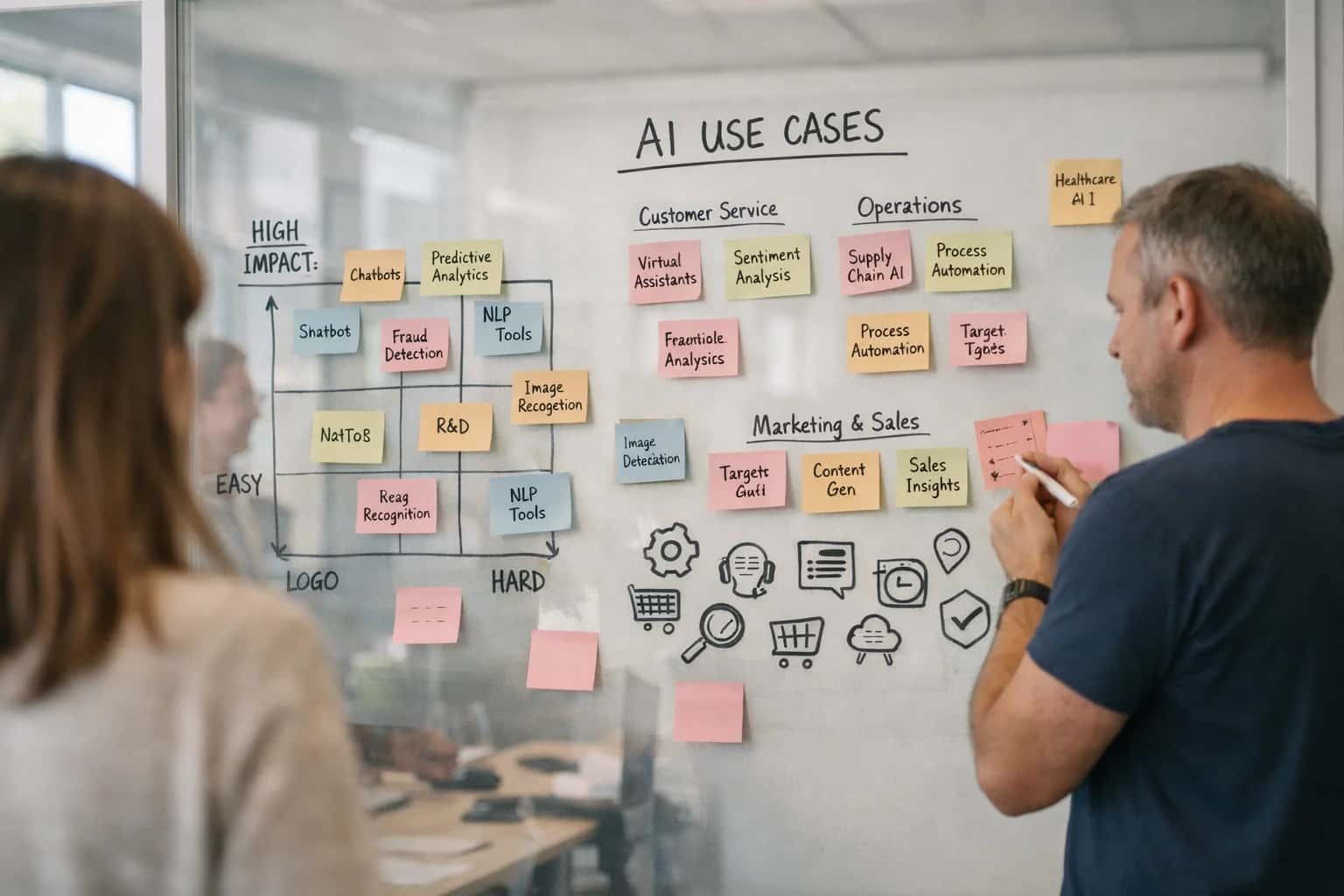
Real-Time Defect Detection in Semiconductor Manufacturing
Deploy edge AI for microscopic wafer inspection to identify defects during production, preventing yield loss and reducing rework costs by up to 90%.
THE PAIN POINT
What is Real-Time Defect Detection in Semiconductor Manufacturing Used For?
In the high-stakes world of semiconductor fabrication, microscopic defects on a wafer can lead to catastrophic yield loss and multi-million dollar scrap costs. Traditional inspection methods are too slow and prone to human error, creating a critical bottleneck.
The AI fix is in-line, real-time vision. By deploying optimized computer vision models directly on edge AI systems within the fab, every wafer is scanned at production speed. Defects are identified and classified in milliseconds, triggering immediate alerts or automated rejection. This shifts quality assurance from a cost center to a profit protector, directly boosting Overall Equipment Effectiveness (OEE) and preventing the costly rework of advanced nodes. For a deeper dive into industrial applications, explore our insights on Edge-Based Quality Inspection on Assembly Lines.
BUSINESS JUSTIFICATION
Common Use Cases for Edge AI in Wafer Inspection
Edge AI transforms semiconductor quality control from a lagging cost center into a real-time strategic asset. By processing data at the source, manufacturers can prevent yield loss, accelerate production, and secure a competitive edge.
01
Zero-Latency Defect Classification
Traditional cloud-based inspection creates a critical delay between detection and classification, allowing defective wafers to progress through the line. Edge AI runs microscopic defect classification models directly on the inspection tool, enabling real-time sorting. This prevents defective wafers from consuming valuable downstream processing resources.
- Real-World Impact: A leading foundry reduced its scrap rate by 18% by halting processing on wafers with critical defects identified in under 50 milliseconds.
- ROI Driver: Directly protects the multi-million dollar value of each production batch by stopping waste at the source.
< 50 ms
Decision Latency
18%
Scrap Reduction
02
In-Line Process Window Control
Subtle variations in etch, deposition, or lithography processes can drift over time, leading to parametric yield loss. Edge AI monitors hundreds of inline metrology signals in real-time, identifying drift patterns before they cause defects.
- Real-World Example: An analog chip manufacturer uses edge inference to adjust plasma etch parameters on-the-fly, maintaining process capability (Cpk) above 1.67. This eliminated a weekly manual calibration step, saving 200+ engineering hours monthly.
- Business Value: Ensures consistent, high-yield production, directly translating to higher revenue per tool and reduced rework costs.
1.67+
Sustained Cpk
03
Root Cause Analysis & Excursion Prevention
When a defect spike occurs, identifying the root cause—whether a specific tool, chamber, or recipe—is a race against time. Edge AI deployed across the fab floor correlates defect signatures with tool sensor data in real-time.
- How It Works: Anomaly detection models flag a defect pattern and instantly query edge nodes on upstream tools. The system pinpoints the faulty chamber within minutes, not days.
- CIO Justification: Reduces Mean Time to Recovery (MTTR) by over 70%, preventing multi-day production excursions that can cost millions in lost output. This capability is foundational for high-mix manufacturing.
70%
Faster MTTR
04
Data Sovereignty & IP Protection
Sending high-resolution wafer imagery to the cloud for analysis creates significant data egress costs and exposes critical intellectual property. Edge AI performs all analysis locally, sending only anonymized metadata and alerts.
- Strategic Advantage: Protects proprietary design patterns and process recipes from external exposure, a key concern for fabs serving defense or automotive sectors.
- Cost Savings: Eliminates terabytes of daily image transfer, reducing cloud storage and bandwidth costs by an estimated $250k+ annually for a medium-scale fab. This aligns with the principles of Sovereign AI Infrastructure.
$250K+
Annual Cost Avoidance
05
Predictive Yield Modeling
Final wafer yield is a lagging indicator, discovered only at the end of a 60-90 day cycle. Edge AI creates a real-time yield prediction by aggregating and analyzing defect maps and parametric data from each process step as the wafer moves through the line.
- Business Intelligence: Provides fab managers with a daily predicted yield for lots in process, enabling proactive capacity planning and customer communication.
- ROI Case: A memory chip maker uses these predictions to dynamically re-prioritize lots based on customer urgency and predicted value, improving on-time delivery for high-margin products by 15%.
15%
On-Time Delivery Lift
06
Legacy Tool Modernization
Retrofitting older inspection and metrology tools with edge AI inference pods extends their useful life and capabilities without a full capital replacement. This delivers advanced analytics at a fraction of the cost of new equipment.
- Implementation Path: A compact edge inference appliance connects to the tool's data port, hosting modern computer vision models that the original vendor does not support.
- Financial Justification: Achieves 80% of the capability of a new $2M tool for less than $200k in edge hardware and software, delivering an ROI in under 6 months. This is a core tactic for Smart Manufacturing and Industry 5.0 Integration.
< 6 mo
ROI Payback
REAL-TIME DEFECT DETECTION
How It Works: The Edge AI Implementation Architecture
In semiconductor manufacturing, a single microscopic defect can scrap a wafer worth thousands of dollars. This use case details how Edge AI architecture transforms quality control from a slow, reactive process into a real-time, preventative system.
The Pain Point is yield loss. Traditional inspection relies on offline, centralized systems where high-resolution images are sent to a cloud server for analysis. This creates a latency of minutes to hours between detection and the production line stoppage. By then, hundreds of defective wafers may have been processed, leading to massive scrap costs, expensive rework, and delayed time-to-market. The inability to act instantly turns a quality issue into a financial hemorrhage.
The AI Fix deploys optimized computer vision models directly on inference engines at the microscope. Images are analyzed in milliseconds, enabling real-time classification of defects—scratches, particles, pattern irregularities. The system triggers an immediate alert to halt the affected tool. This architecture, detailed in our guide to Edge AI and Real-Time Local Inference, prevents defect propagation, boosting yield by 5-10% and delivering a clear ROI through reduced waste and higher throughput, as seen in our Smart Manufacturing solutions.
COST OF INACTION
ROI Calculator: Cost Savings from Early Defect Detection
This table quantifies the financial impact of detecting a single defect at different stages of the semiconductor manufacturing process. Early detection with edge AI prevents the compounding costs of processing defective wafers.
| Process Stage | Traditional Sampling | Inline Vision Systems | Edge AI Real-Time Detection |
|---|---|---|---|
Detection Point | End-of-Line (EOL) Test | Post-Lithography | During Process |
Typical Detection Latency | 2-4 weeks | 24-48 hours | < 1 second |
Wafers at Risk of Scrap | 100-500 wafers | 10-50 wafers | 1 wafer |
Avg. Cost per Scrapped Wafer | $5,000 - $50,000 | $5,000 - $50,000 | $5,000 - $50,000 |
Potential Yield Loss per Defect | 0.5% - 2.5% | 0.05% - 0.25% | < 0.01% |
Re-work Possible | |||
Annualized Savings per Fab Line* | Baseline | $2M - $10M | $10M - $50M+ |
Enabling Efficiency, Speed & Accuracy
Intelligent Analysis, Decision & Execution
We build AI systems for teams that need search across company data, workflow automation across tools, or AI features inside products and internal software.
Talk to Us
Search across company data
Give teams answers from docs, tickets, runbooks, and product data with sources and permissions.
Useful when people spend too long searching or get different answers from different systems.
Enterprise searchRAGPermissions
Read more
Automate internal workflows
Use AI to route work, draft outputs, trigger actions, and keep approvals and logs in place.
Useful when repetitive work moves across multiple tools and teams.
AI agentsWorkflow automationGovernance
Read more
Add AI to products and internal tools
Build assistants, guided actions, or decision support into the software your team or customers already use.
Useful when AI needs to be part of the product, not a separate tool.
AI integrationDecision supportModel routing
Read moreREAL-TIME DEFECT DETECTION
Key Implementation Challenges & Mitigations
Deploying AI for real-time wafer inspection delivers immense ROI but introduces unique technical and operational hurdles. This guide addresses the most common enterprise objections, providing clear mitigation strategies to ensure a successful, scalable implementation.
The primary ROI is yield improvement and cost avoidance. A single defective wafer can cost tens of thousands of dollars in scrapped materials and rework. By catching defects in-line, you prevent bad product from moving downstream, directly boosting yield by 1-3% or more. Secondary ROI comes from reduced manual inspection labor and faster time-to-market through accelerated process qualification. For a typical fab, the payback period for an edge AI system can be under 12 months. To quantify this, we recommend a pilot focused on a single, high-value inspection point to measure defect escape reduction and throughput impact before scaling. Learn more about building a business case in our guide on Outcome-Based AI Service Models and ROI Analytics.

About the author
Prasad Kumkar
CEO & MD, Inference Systems
Prasad Kumkar is the CEO & MD of Inference Systems and writes about AI systems architecture, LLM infrastructure, model serving, evaluation, and production deployment. Over 5+ years, he has worked across computer vision models, L5 autonomous vehicle systems, and LLM research, with a focus on taking complex AI ideas into real-world engineering systems.
His work and writing cover AI systems, large language models, AI agents, multimodal systems, autonomous systems, inference optimization, RAG, evaluation, and production AI engineering.
LinkedIn
Limited slotsGet a Free AI Consultation
Partnered with leading AI, data, and software stack.


How We Work
Custom AI workflows for your Business
One-fit-all AI don't work for modern businesses. At Inferensys, we aim to understand your business & custom requirements; which we use to define most efficient agentic workflows, the data, and the tools for your business.
01
Review the use case
We understand the task, the users, and where AI can actually help.
Read more02
Pick the right approach
We define what needs search, automation, or product integration.
Read more03
Build the first useful version
We implement the part that proves the value first.
Read more04
Improve from there
We add the checks and visibility needed to keep it useful.
Read moreThe first call is a practical review of your use case and the right next step.
Talk to Us